- 您现在的位置:买卖IC网 > Sheet目录341 > MAX6971AUG+T (Maxim Integrated)IC LED DRIVER LINEAR 24-TSSOP
16-Port, 36V Constant-Current LED Driver
CLK is the serial-clock input, which shifts data at DIN
into the MAX6971 16-bit shift register on its rising edge.
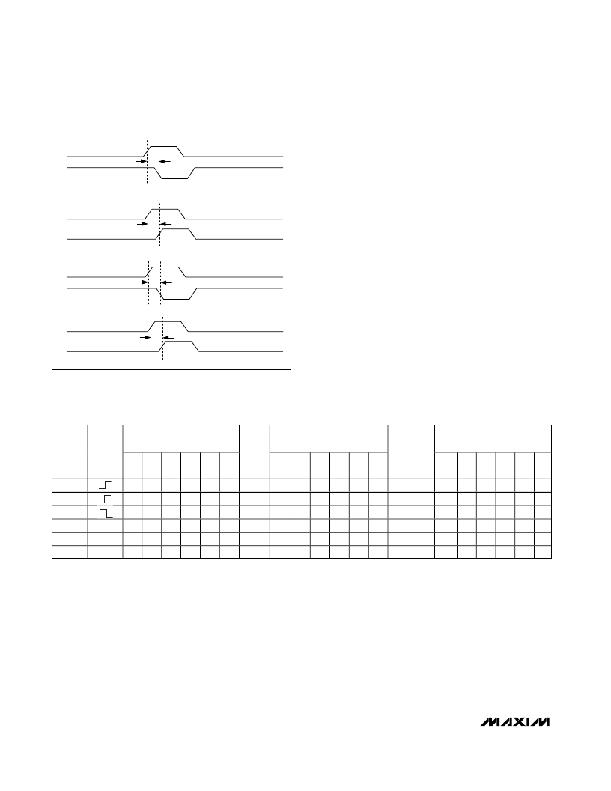
LE
OUT_
LE
OUT_
t LRF
t LRR
LE is the latch load input of the MAX6971 that transfers
data from the MAX6971 16-bit shift register to its 16-bit
latch when LE is high (transparent latch), and latches
the data on the falling edge of LE (Figure 2).
The fourth input provides output-enable control of the
output drivers. OE is high to force outputs
OUT0 –OUT15 high impedance, without altering the
contents of the output latches, and low to enable out-
puts OUT0 –OUT15 to follow the state of the output
latches.
CLK
OUT_
t CRF
OE is independent of the operation of the serial inter-
face. Data can be shifted into the serial-interface shift
register and latched, regardless of the state of OE .
DOUT is the serial-data output, which shifts data out
CLK
t CRR
from the MAX6971’s 16-bit shift register on the rising
edge of CLK. Data at DIN is propagated through the
shift register and appears at DOUT 16 clock cycles later.
OUT_
Figure 3. LE and CLK to OUT_ Timing
Table 1. 4-Wire Serial-Interface Truth Table
SERIAL
DATA
INPUT
DIN
CLOCK
INPUT
CLK
D 0
SHIFT-REGISTER
CONTENTS
D 1 D 2 … D n-1 D n
LOAD
INPUT
LE
D 0
LATCH CONTENTS
D 1 D 2 … D n-1 D n
BLANKING
INPUT
OE
D 0
OUTPUT CONTENTS
D 1 D 2 … D n-1 D n
H
L
X
H
L
R 0
R 1
R 1
R 1
R 2
R 2
R 2
… R n-2 R n-1
… R n-2 R n-1
… R n-1 R n
—
—
—
—
—
—
—
—
—
—
—
—
—
—
—
—
—
—
—
—
—
—
—
—
—
—
—
—
—
—
—
—
—
—
—
—
—
—
—
—
—
—
—
—
X
X
X
…
X
X
H
R 0
R 1
R 2
— R n-1 R n
—
—
—
—
—
—
—
—
—
P 1
P 2
P 3
… P n-1 P n
L
P 0
P 1
P 2
… P n-1 P n
L
P 0
P 1
P 2
… P n - 1 P n
—
—
—
—
—
— — —
—
X
X
X
…
X
X
H
Hi-Z Hi-Z Hi-Z … Hi-Z Hi-Z
L = Low-logic level.
H = High-logic level.
X = Don’t care.
P = Present state.
R = Previous state.
Hi-Z = High impedance.
8
_______________________________________________________________________________________
发布紧急采购,3分钟左右您将得到回复。
相关PDF资料
MAX6974ATL+
IC LED DRIVER LINEAR 40-TQFN
MAX6977AAE+
IC LED DRIVER LINEAR 16-SSOP
MAX6978AUE+
IC LED DVR CONST-CURR 16TSSOP
MAX6979AUG+
IC LED DRIVER LINEAR 24-TSSOP
MAX6983AUG+T
IC LED DRIVER LINEAR 24-TSSOP
MAX71020AEUI+
IC ENERGY METER 1PH 28TSSOP
MAX7302ATE+
IC LED DRIVER LINEAR 16-TQFN
MAX7307AUB+T
IC LED DRIVER LINEAR 10-UMAX
相关代理商/技术参数
MAX6971AUG-T
功能描述:LED显示驱动器 RoHS:否 制造商:Micrel 数位数量:5 片段数量: 安装风格:SMD/SMT 封装 / 箱体:PLCC-44 工作电源电压:4.75 V to 11 V 最大电源电流:10 mA 最大工作温度:+ 85 C 最小工作温度:- 40 C 封装:Tube
MAX6971EVKIT+
功能描述:LED 照明开发工具 Evaluation Kit for the MAX6971 RoHS:否 制造商:Fairchild Semiconductor 产品:Evaluation Kits 用于:FL7732 核心: 电源电压:120V 系列: 封装:
MAX6972ATJ
制造商:Maxim Integrated Products 功能描述:16-OUTPUT PWM LED DRIVERS FOR MESSA - Rail/Tube
MAX6972ATJ+
制造商:Maxim Integrated Products 功能描述:LED DRVR 16SEGMENT 3.3V 32TQFN EP - Rail/Tube
MAX6972ATJ+T
制造商:Maxim Integrated Products 功能描述:LED DRVR 16SEGMENT 3.3V 32TQFN EP - Tape and Reel
MAX6972ATJ-T
制造商:Maxim Integrated Products 功能描述:16-OUTPUT PWM LED DRIVERS FOR MESSA - Tape and Reel
MAX6972EVKIT
制造商:Maxim Integrated Products 功能描述:16-OUTPUT PWM LED DRIVERS FOR MESSA - Rail/Tube
MAX6973ATJ
功能描述:LED显示驱动器 RoHS:否 制造商:Micrel 数位数量:5 片段数量: 安装风格:SMD/SMT 封装 / 箱体:PLCC-44 工作电源电压:4.75 V to 11 V 最大电源电流:10 mA 最大工作温度:+ 85 C 最小工作温度:- 40 C 封装:Tube
